A flip-flop in digital electronics is formally defined as "A bistable device with synchronous inputs that changes state only at specified transitions of a clock signal" (IEEE Standard 91/1984)
In general, flip-flops are fundamental components in digital electronics, capable of functioning as 1-bit memory storage devices. Unlike combinational logic gates, flip-flops have the unique ability to store state information (0 or 1, low or high) and maintain this stored state indefinitely until changed, all with synchronized operation using a clock signal.
If this sounds confusing right now, don't worry! By the end of this article, you'll understand everything clearly with simple explanations and real-world examples.
What is a flip-flop and how does it work?
A flip-flop is a fundamental digital circuit designed to store a single bit of data, serving as a critical memory element in electronics. It maintains one of two stable states (0 or 1) and transitions between them based on input signals and a clock pulse. There are many types of flip-flops, such as SR (Set-Reset), D (Data), JK, and T (Toggle) flip-flops and each has distinct input-output functionalities. We will get in-depth into each of them but for simple understanding, a D flip-flop captures the input value at the clock’s edge and holds it until the next cycle, ensuring precise data retention. Essential in sequential logic, flip-flops are integral to registers, counters, and memory units in microprocessors and digital systems, enabling synchronized and reliable operation.
Flip-flops operate by processing input signals through logic gates, with state changes synchronized by a clock signal to ensure stability and predictability. For example, in a D flip-flop, the data input is sampled only when the clock triggers, storing the value in a feedback loop until the next clock edge. Similarly, an SR flip-flop uses set and reset inputs to toggle states, while a JK flip-flop offers enhanced flexibility by resolving indeterminate states. This clock-driven mechanism prevents erratic behavior, making flip-flops ideal for applications requiring precise timing, such as in CPUs and memory modules. By maintaining and updating data in a controlled manner, flip-flops form the backbone of modern digital circuit design.
Difference between flip-flop and latch
When learning about flip-flops, it’s essential to mention latches as well—and there’s a good reason. The evolution of digital electronics typically follows this path:
Transistors → Logic Gates → Latches → Flip-Flops
This progression is why flip-flops and latches are often compared, even though they serve different purposes in circuit design.
Put simply, flip-flops are an advanced form of latches. Both can store a single bit of data, but,
Flip-flops are edge-triggered and change states based on a synchronous clock signal.
Latches are level-sensitive, meaning their output changes whenever the input signal is active.
The main challenge with using multiple latches is synchronization. Since latches respond immediately to input changes, a slight delay in signal arrival (like due to varying wire lengths) can lead to timing errors. In high-speed circuits, even nanosecond-level differences can cause problems.
Flip-flops solve this issue by ensuring all data changes happen only at the clock edge, making them perfect for synchronized operations.
With the above comparison chart, I’m sure you'll understand the difference between the two more clearly. With this, let's move on to the types of flip-flops, along with practical demonstrations.
Types of Flip-Flops in Digital Electronics
Although flip-flops evolved from latches, the Flip-Flop itself has some types to make it fit in certain applications. As I said, each single type was an evolution from another with a few improvements. So, without wasting any time, let's jump straight away into the types of flip-flops,
Here are the four primary types of Flip-Flops, which are
SR Flip-Flop
The SR (Set-Reset) Flip-Flop is the most basic and commonly used type of flip-flop, and it’s the foundation for more advanced types like D, JK, and T. It has two inputs: S (Set) and R (Reset). When S = 1, the output is set to 1. When R = 1, it resets to 0. If both S and R are 0, the output simply holds the previous state. But if S = R = 1, it enters an invalid state (also called the race around condition), which must be avoided in real-world circuits.
Unlike latches that respond to input levels, the SR Flip-Flop is edge-triggered, meaning it only reacts at the rising or falling edge of the clock signal. This makes it more reliable for timed operations in sequential circuits.
Also, keep in mind: most flip-flops (and logic ICs) are rising edge-triggered, while falling edge or dual-edge triggered types are rare and used in specific designs. That’s why we generally call them edge-triggered—because either edge could be used, depending on the application.
SR Flip-Flops are often used in basic control systems, like
Turning a relay ON or OFF with logic signals,
Simple memory storage where only a few states are needed, like in reset/start switches, push button debouncing.
Simple status flags.
Symbol & Truth Table of SR Flip-Flop
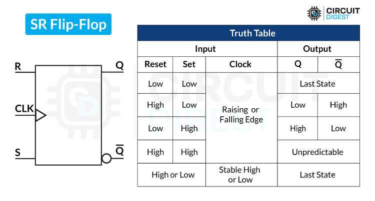
Above, you can see the symbol, along with the truth table. After undergoing some detailed research, we arrived at this truth table.
To make this simple to understand, I’ve used straightforward terms here:
No Change (S = R = 0): The flip-flop retains its previous state.
Set (S = 1, R = 0): Output Q becomes '1' (Set).
Reset (S = 0, R = 1): Output Q becomes '0' (Reset).
Invalid State (S = R = 1): Both outputs (Q and Q̅) may become '1', leading to instability. This condition is prohibited in most designs.
SR Flip-Flop Circuit Working
One of the simplest ways to implement an SR flip-flop is using NAND gates.
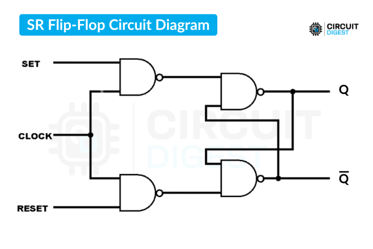
Above, you can see the basic circuit diagram of an SR flip-flop made using a combination of NAND gates. You can use any NAND IC, and the result will be the same. Here, we are using four NAND gates to construct the SR flip-flop.
The working is simply a combinational output of the logic gates. If you spend some time mapping the values for each individual logic gate, you should be able to understand it clearly.
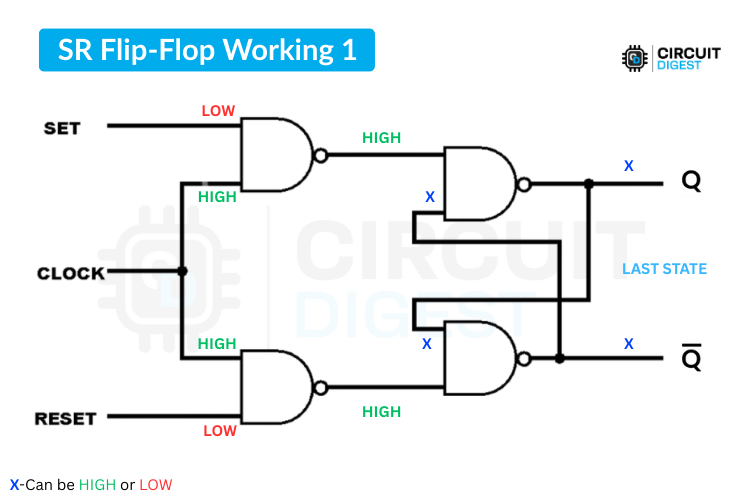
According to the truth table, if we initially keep both the Set and Reset inputs LOW, the output will remain in its last state. I would like to add a note that this behavior might vary depending on the setup, especially between simulation and real hardware implementation.
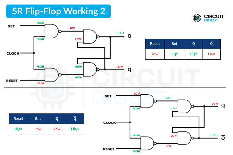
If I make the Set pin HIGH while keeping the Reset pin LOW, that will eventually make Q HIGH and Q̅ LOW. Conversely, if the Reset pin is kept HIGH and the Set pin LOW, you will get LOW at Q and HIGH at Q̅.
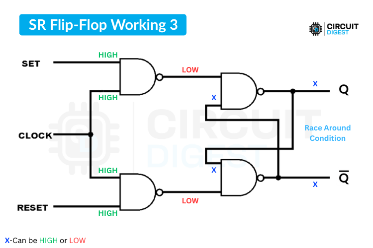
Furthermore, if we keep both Set and Reset HIGH, the output will be unpredictable. In more technical terms, a race-around condition will occur, which should be avoided. To overcome that issue, the SR flip-flop was upgraded to a D flip-flop.
Practical Demonstration of SR Flip-Flop
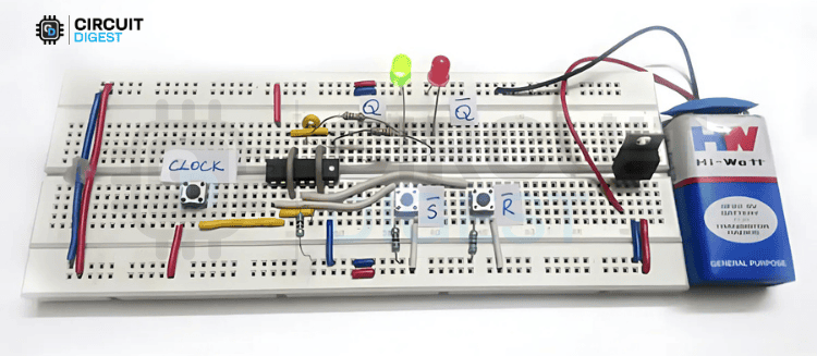
To learn the SR flip-flop in a more practical way, you can refer to the article SR Flip-Flop with NAND Gates: Circuit, Truth Table and Working, which covers the SR flip-flop concept, its truth table, a list of components required, the circuit diagram with explanation, and the working of the SR flip-flop using NAND gates.
How to make SR flip-flop using NAND gates?
An SR (Set-Reset) flip-flop can be effectively built using NAND gates, as shown in the provided circuit diagram, which utilizes four 7400-series NAND gates. The 7400 chip contains four 2-input NAND gates, each with inputs (e.g., pins 1 and 2) and an output (pin 3). In this setup, two NAND gates form the core latch, while the other two act as input conditioners with the clock signal. The inputs S (Set) and R (Reset) are fed into the first pair of NAND gates alongside the clock signal, ensuring that state changes occur only on clock pulses. The outputs of these gates connect to the second pair, which are cross-coupled to create the latch, producing the Q and Q' (complementary) outputs. This configuration ensures the flip-flop stores a bit of data, setting Q to 1 when S is active or resetting Q to 0 when R is active, all synchronized by the clock.
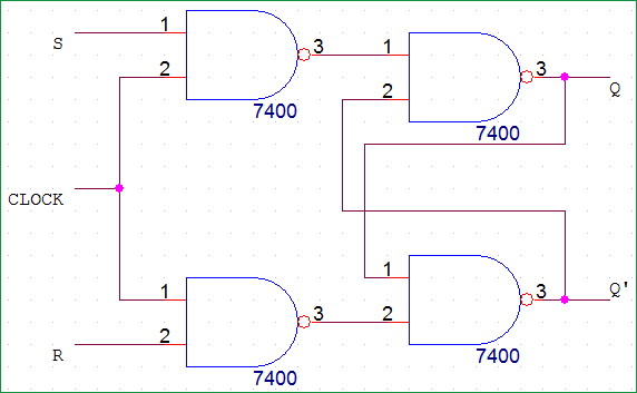
In the diagram, the clock signal enables the flip-flop to update its state only when active (typically high). When the clock is high, the first NAND gate (top left) processes the S input, and the second NAND gate (bottom left) processes the R input. These outputs feed into the cross-coupled NAND gates (right side), which form the latch. If S is 1 and R is 0, the latch sets Q to 1 and Q' to 0; if R is 1 and S is 0, it resets Q to 0 and Q' to 1. When both S and R are 0, the latch holds its previous state, and both being 1 is an invalid condition for an SR flip-flop, as it leads to instability. The use of NAND gates ensures that the circuit operates reliably, with the clock providing precise control over when the flip-flop updates, making it ideal for applications in sequential logic circuits like registers and counters.
D Flip-Flop
The D Flip-Flop is actually an upgrade of the SR Flip-Flop, specifically designed to overcome its major limitation—the invalid state. Unlike the SR Flip-Flop, which requires two inputs (Set and Reset) and may enter an undefined condition when both are high, the D Flip-Flop simplifies the design by using just one input, the D (Data) input.
The operation is straightforward, whatever value is applied to the D input gets stored and reflected at the output Q, but only at the triggering edge of the clock signal (usually the rising edge).
Because it cleanly passes the input to the output in a controlled and predictable way, the D Flip-Flop is widely used in digital electronics, especially in applications like Data storage registers, Pipeline registers in CPUs, Buffering systems, Clocked data transfer circuits
Symbol & Truth Table of D Flip-Flop
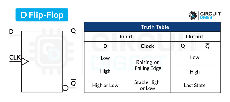
Above, you can see the symbol along with the truth table for the D flip-flop. It is self-explanatory and simple to understand.
In Simple Terms:
At Clock Edge (↑), the flip-flop copies the D input and holds it until the next tick. That is, if we give HIGH, then Q will be HIGH, and vice versa.
Otherwise, the output stays the same as the previous state.
D Flip-Flop Circuit Working
Among many options for implementing a D flip-flop, I’ll go with the NAND gate version to keep it simple.
Below, you can see the circuit diagram of the D flip-flop, which might look similar to the SR flip-flop.

The only difference is that we have used an additional NAND gate as a NOT gate and combined the Set and Reset inputs into a single D input.

Here, as per the combinational logic circuit, Q will be equal to the D input value. If D is HIGH, Q will be HIGH, and Q̅ will be LOW. Similarly, when we provide LOW to the D input, Q will be LOW, and Q̅ will be HIGH. This all happens only at the rising or falling edge of the clock pulse.
If the clock pulse remains at the same logic level (either HIGH or LOW), then regardless of the D input, Q and Q̅ will remain the same as their last state.
Practical Uses of the D Flip-Flop
The D flip-flop is widely used in digital electronics for reliable data storage and synchronization. It forms the core of shift registers, enabling serial-to-parallel data conversion in communication systems. In microprocessors, D flip-flops are essential for building registers to hold temporary data during processing. They’re also used in counters, facilitating frequency division and event sequencing in clocks and timers. Additionally, D flip-flops ensure synchronized data transfer in memory units, preventing timing errors. Their ability to capture and hold data on clock edges makes them indispensable in sequential logic circuits.
If you want to explore the D Flip-Flop in a more practical way, check out the article D Type Flip-Flop: Circuit, Truth Table and Working. It covers the D Flip-Flop basics, truth table, logic gate representation, list of components required, circuit diagram with explanation, a practical demonstration, and even a video to help you understand better.
JK Flip-Flop
The JK Flip-Flop comes with a bit of history behind its name. The most common explanation is that it was just a naming choice used by an engineer in his documentation, maybe based on initials or just random letters that stuck around. Whatever the reason, this flip-flop became popular because it fixed a major issue in the SR Flip-Flop.
It has two inputs, J and K, which function similarly to the Set and Reset inputs in an SR flip-flop, but with a smart upgrade. When both J and K are held HIGH, instead of entering an invalid or unstable state (as seen in the SR flip-flop), the JK flip-flop simply toggles its output. This means if Q is currently LOW, it becomes HIGH, and if Q is HIGH, it becomes LOW. This automatic flipping behavior is what makes the JK flip-flop particularly useful and reliable in sequential circuits.
Because of this, the JK Flip-Flop is perfect for things like counters, digital clocks, and frequency dividers, where the circuit needs to switch states on its own in a clean and timed manner.
Symbol and Truth Table of the JK Flip-Flop

With the above symbol and truth table, you can understand the concept behind the JK flip-flop.
Just like the SR flip-flop, the combinations LOW-LOW, HIGH-LOW, and LOW-HIGH behave the same way. However, if both the J and K inputs are set to HIGH, you will observe a continuous state toggle with each clock pulse. So, let’s move on to the working part to understand it more clearly.
Working Explanation of JK Flip Flop
Like SR and D, it is also possible to implement a JK flip-flop using NAND gates. And that will be appropriate to learn the behavior easily.
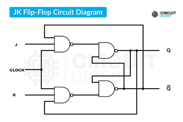
Above, you can see the circuit diagram, but with a difference, it uses a 3-input NAND gate. So, it looks a little complex, but it’s actually quite easy.
If you're someone like me who tries to test the circuit using any simulation software like Proteus or Logisim, you might face difficulties in getting the proper output—I did too.
This flip-flop is difficult to simulate with its current combination. So, after some research, I found the circuit diagram below to work well for simulation. This was simulated using Proteus, and it replicates the same JK logic.
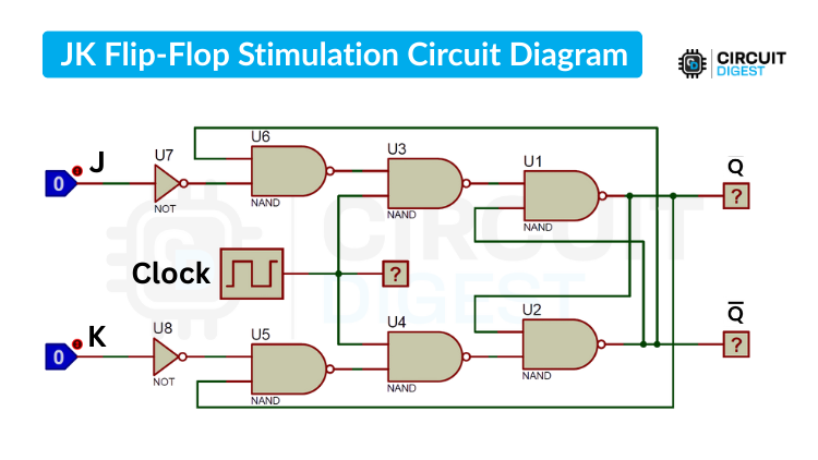
This is because, in real-world situations, there are pull-ups and pull-downs responsible for maintaining the active LOW or active HIGH state. But in simulation, it seems to lack such features. Adding them manually also didn’t work on my side.
With this, we can move to the explanation of the working.
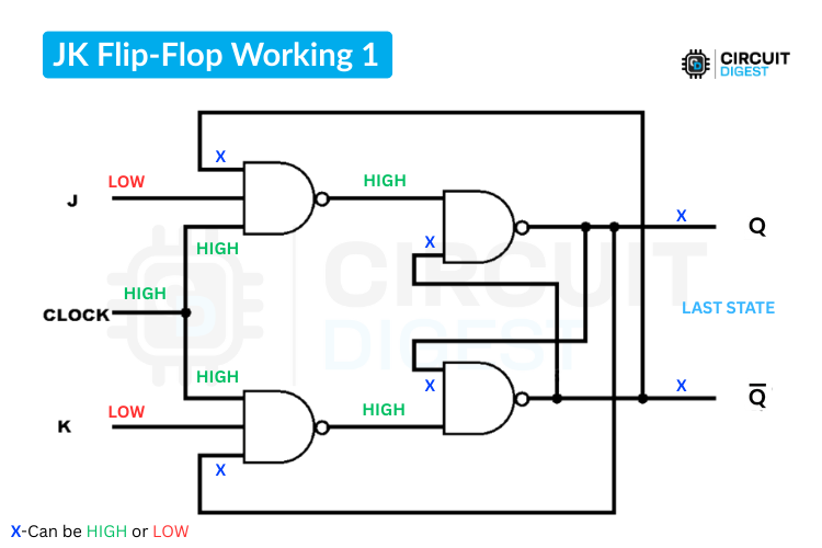
Here, most of the logic is similar to the SR flip-flop, which means if you keep both inputs LOW, it will remain in the last state.
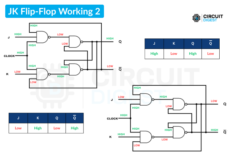
And if the J input is kept HIGH and the K is kept LOW, the output Q will be HIGH and Q̅ will be LOW.
Vice versa, if the J input is kept LOW and the K input is kept HIGH, the expected output will be Q LOW and Q̅ HIGH.
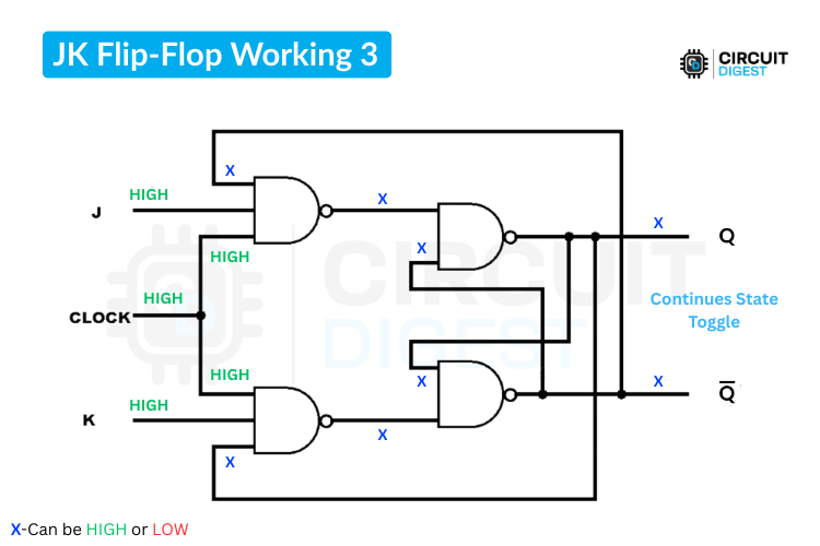
But in the case where both inputs are HIGH, the output will continuously toggle with each clock pulse.
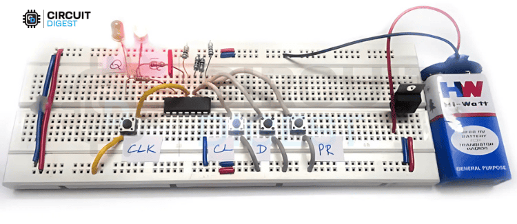
Hope you got to know about the JK flip-flop. Now, in case you are looking to implement this in real-time hardware, we can still make it simple by using dedicated JK flip-flop ICs like 7473, which is often known as MC74HC73A, SN74LS73A, etc. By using this, it’s much easier to implement the JK flip-flop.
Simple explanation of JK flip-flop with Circuit
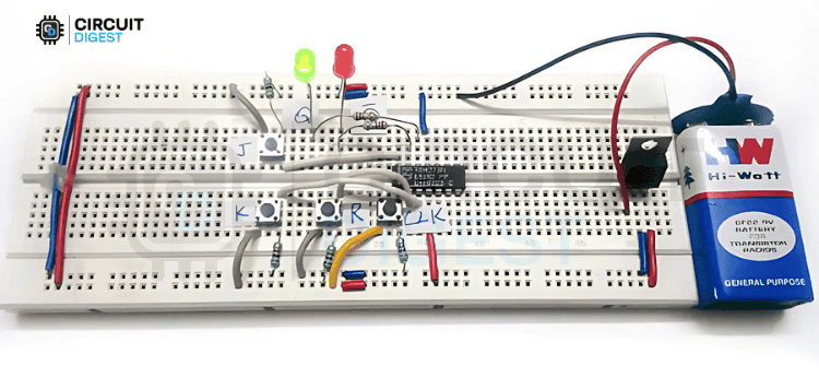
To explore the representation of JK Flip-Flop using logic gates, a list of components required, the circuit diagram with explanation, and a practical demonstration with working, you can check out the article: JK Flip-Flop: Circuit, Truth Table and Working.
T Flip-Flop
The T Flip-Flop, also known as the Toggle Flip-Flop, is actually a simplified version of the JK Flip-Flop. In fact, it’s like taking a JK Flip-Flop and tying both the J and K inputs together. So instead of two inputs, it has just one—called T (for Toggle).
The working is super simple,
When T = 0, nothing happens. The output stays the same.
When T = 1, the output continuously toggles. IE: If Q = 0, it becomes 1; if Q = 1, it becomes 0, and this cycle repeats on each Clock pulse.
That’s it. This flip-flop is all about flipping the state when told to do so.
Because of its simplicity, the T Flip-Flop is commonly used in binary counters, toggle switches, and control circuits, especially where you want to alternate states with each clock pulse. It’s a neat little component that turns a basic input into reliable, timed output transitions.
Symbol & Truth Table of the T Flip-Flop
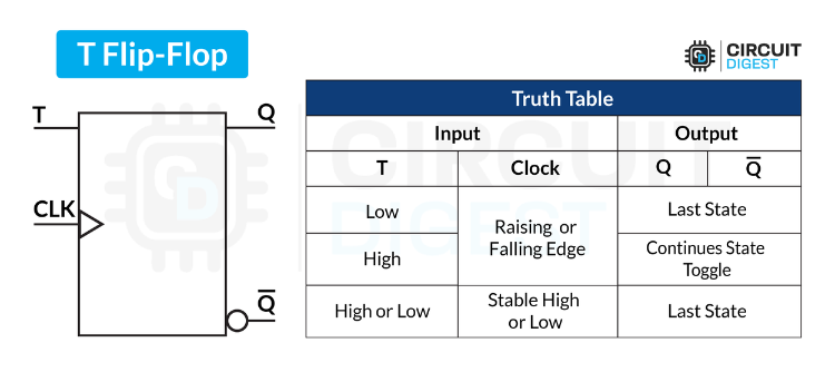
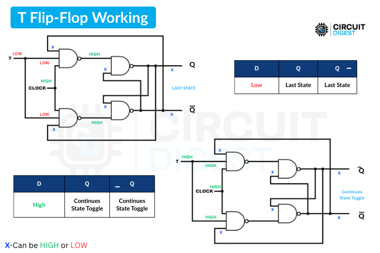
Above you can see the symbol and the truth table for the T Flip-Flop. The T Flip-Flop has just one input, T, and it works based on clock edges—usually the rising edge.
If T is set LOW, the output doesn’t change, no matter how many clock pulses come in. It just holds the previous state.
But when T is set HIGH, the magic happens—on every rising edge of the clock, the output continuously toggles. That means if the current output (Q) is LOW, it becomes HIGH, and if it’s HIGH, it becomes LOW.
T Flip-Flop Circuit Working
As you know, this T Flip-Flop is the extended version of the JK Flip-Flop. Simply tying the J and K inputs of the JK Flip-Flop to the T input makes the T Flip-Flop. Below you can see the circuit diagram of the T Flip-Flop.
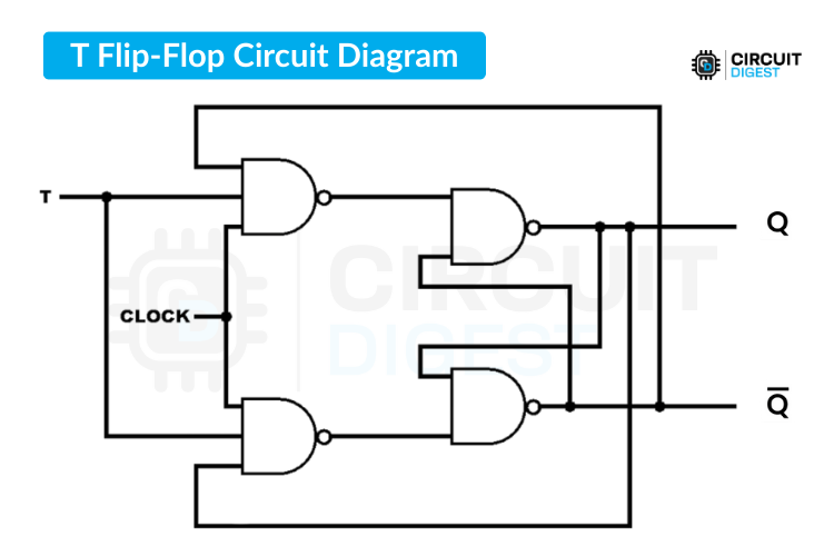
As we already discussed in the JK working section, simulating the same is not easy. I tried different combinations, but finally, it was only possible using the direct JK Flip-Flop IC. So, if you need to do a simulation, you can check it out using the 7473 JK Flip-Flop IC.
Above you can see the general working of the T Flip-Flop’s combinational logic circuit. As we already discussed, when T is LOW (0), the output stays in its last state, no matter how many clock pulses you give. But when T is HIGH (1), the output toggles on every rising edge of the clock—so if Q was 0, it becomes 1, and if it was 1, it becomes 0.
Just like the JK Flip-Flop, we can use the 7473 IC for demonstrating the T Flip-Flop.
Practical Demonstration of the Toggle Flip-Flop
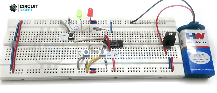
To dive deeper into the T Flip-Flop, check out the article T Flip-Flop: Circuit, Truth Table and Working. It explains the logic diagram, truth table, and excitation table, compares D and T flip-flops, shows how to convert between D, T, and JK flip-flops, lists the components required, and includes the circuit diagram, working explanation, a practical demo, and even a video to help you understand it clearly.
Comparison between the types of flip-flop
Hope you understand all the types of Flip-Flop Individually in the above sections. Now lets go through a direct brief comparison between each type of flip-flop.
Remember,
SR Flip-Flop is basic but can become unstable when both inputs are HIGH.
D Flip-Flop is ideal for precise data latching, what goes in comes out on clock.
JK Flip-Flop fixes SR's flaws and adds a toggle feature, great for counters.
T Flip-Flop is perfect for flipping states, used widely in frequency division.
Projects on Flip-Flop
These projects offer practical insights into flip-flop applications in digital electronics, helping to understand their use in memory storage, timing circuits, counters, and data synchronization in simple systems.

SR Flip-Flop with NAND Gates: Circuit, Truth Table and Working
Learn how to design an SR flip-flop circuit using NAND gates. This article covers the circuit diagram, working principles, and truth table for a better understanding of SR flip-flops in digital electronics.

T Flip-Flop: Circuit, Truth Table and Working
Learn about T Flip-Flop circuits, including their truth table, working principles, and applications. Explore how this type of flip-flop is used in digital electronics for toggling operations and building counters, with practical circuit examples and clear explanations.

JK Flip-Flop: Circuit, Truth Table and Working
Explore the JK Flip-Flop, its truth table, working principles, and circuit design. Explore its applications in digital electronics, including its use in counters and toggle circuits. Understand how this versatile flip-flop functions with practical examples and clear explanations.

D Type Flip-Flop: Circuit, Truth Table and Working
Understand how the D Flip-Flop works, including its circuit design, truth table, and practical uses. Learn its importance in memory storage and data synchronization with simple explanations and diagrams.